Productive LED Wafer Marking
Today’s LED technology relies considerably on the use of Gallium Nitride on Silicone (GaN on Si) wafers. Marking these wafers using diode pumped solid state (DPSS) Nd:YAG lasers has proved a problem, primarily due to the laser source.
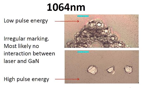
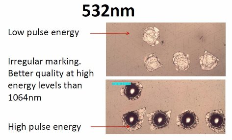
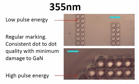
For example, with a 1064 nm infrared laser and even a 532 nm green laser, irregular marking and damage to the GaN layer often occurs. Emitting just 355 nm, ultraviolet has proved to be the solution providing regular marking with consistent dot to dot quality and creating minimum damage to the GaN.


Designed for LED and Semiconductor Marking
The new Innolas IL 1000 LED and Semiconductor Wafer Marking System is available from TLM Laser in a range of different laser types and set-ups, including UV.
Dependent on laser type, the system will achieve optimum process results for various wafer materials such as Gan on Si, GaAS, Ge, SiC, GaP, InP, Sapphire, Quartz and others. Multiple wafer diameters range from 2” to 200mm without requiring mechanical modifications to the system. The system is capable of marking all common types of dot matrix fonts:
- OCR text
- BC412
- SEMI TT-code
The wafer marking system is controlled by an industrial PC using an Intel Pentium processor with 3.06 Ghz. The metal 19” bearing rail unit is designed for rough industrial use and easy maintenance. The powerful software package includes a user friendly operator and engineer interface along with sophisticated diagnostic features for maintenance and service personnel. Options include wafer sorting and SECS/GEM host interface. Customised software solutions are available on request at sales@TLM-laser.com
Diode Pumped Laser System
The IL1000 Series has been developed by Innolas to ensure optimum performance for both material and process requirements. The laser head is axial pumped by high power laser diodes to deliver excellent beam quality and pulse to pulse stability, long durability and low power consumption.
Laser Specifications
|
Wavelength (nm)
|
355/532/1064/10600
|
|
Beam quality
|
1,2
|
|
Average power
|
10 watts @ 5 kHz
|
|
Cooling internal
|
Closed water circuit
|
|
Cooling external
|
Water to water / water to air optional
|
Fully Supported by TLM
Innolas products are available from and fully supported by TLM Laser. One operator training is included and will be carried out at the customer’s facility during installation. Phone support is always available during normal business hours. Spare parts are normally shipped within 24 hours, Monday to Friday.
For further details of the Innolas IL 1000 LED and Semiconductor Wafer Marking System and the full range of Innolas high-end laser systems for industry and research, please contact TLM Laser at sales@TLM-laser.com.