Laser Systems
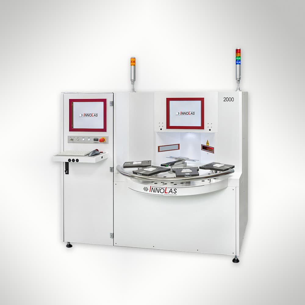
IL 2000
The IL 2000 from InnoLas is a high-precision wafer marking system designed for advanced semiconductor identification. Supporting Nd:YAG and CO2 lasers, it delivers versatile marking options with a throughput of up to 180 wafers per hour.
Laser Type
The IL 2000 supports IR laser sources, including CO2 lasers operating at 10.6 µm and Nd:YAG lasers at 1064 nm. These lasers enable efficient, high-quality marking for a variety of semiconductor materials, ensuring reliability and precision.
The IL 2000 is equipped with UV solid-state Nd:YAG lasers operating at 355 nm. These lasers deliver precise, high-contrast markings with minimal heat impact, ideal for delicate wafer materials and fine-detail applications.
The IL 2000 features green solid-state Nd:YAG lasers operating at 532 nm. These lasers provide excellent beam quality for precise and high-contrast marking on a range of semiconductor materials.

Laser Systems
Semiconductor Processing
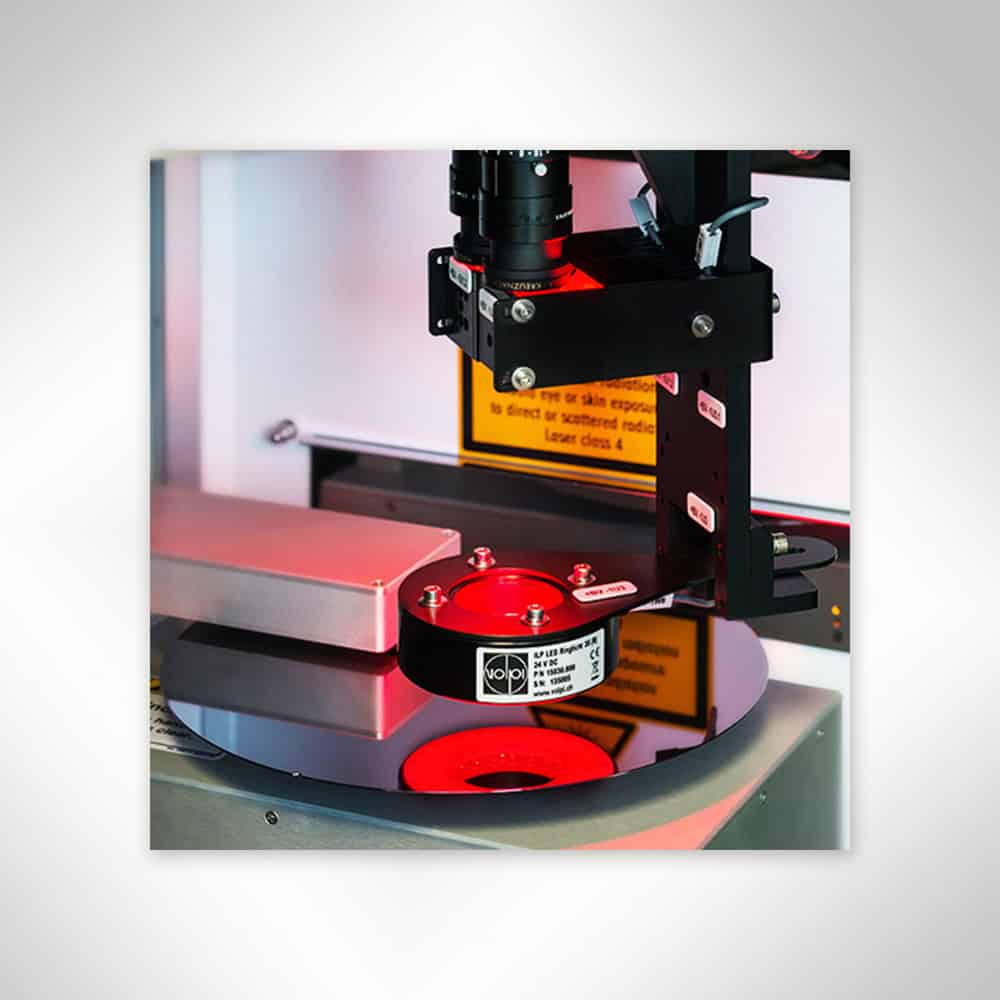
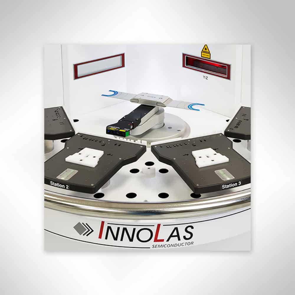
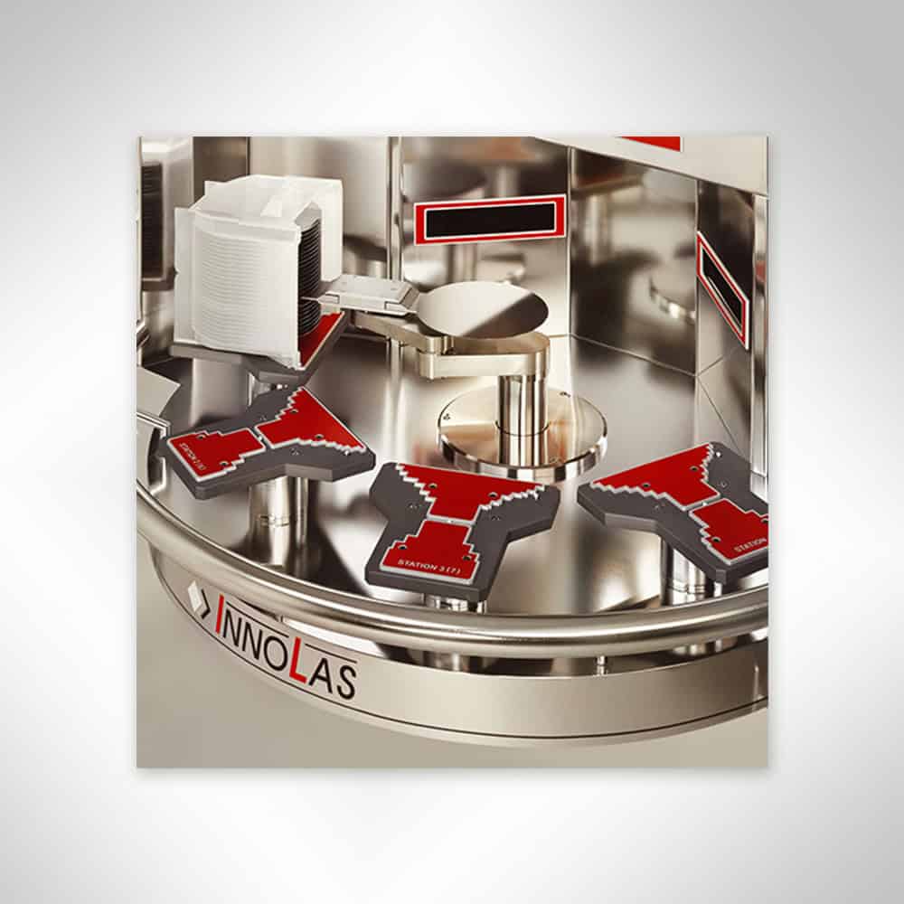
The IL 2000 by InnoLas Semiconductor is a cutting-edge wafer marking system designed for high-throughput semiconductor manufacturing. It supports Nd:YAG lasers at 355 nm (UV), 532 nm (Green), and 1064 nm (IR), as well as CO2 lasers at 10.6 µm (IR), providing flexibility for various materials and marking requirements. The system features high-precision F-Theta lenses and digitally controlled galvo heads, ensuring consistent, high-quality markings. Offering a dot depth range of 0.1 µm to 100 µm and dot diameters between 25 µm and 150 µm, it accommodates SEMI-standard fonts, barcodes, and 2D codes. The IL 2000 supports wafer sizes from 2 inches to 200 mm and features a single-arm robot with double end-effector for efficient handling. With a throughput of up to 180 wafers per hour, advanced opto-mechanical alignment, and customizable serialization options, the IL 2000 is an ideal solution for high-volume semiconductor production.
Send a Product Request
Product Form
Contact form for product pages
"*" indicates required fields
Laser Cleaning
Related Laser Cleaning Systems
Answering Your Questions
Frequently Asked Questions
Both laser marking and wafer sorting are integral to maintaining high-quality standards in semiconductor production. Laser marking provides permanent identification of each component, enabling traceability and facilitating the tracking of products throughout their lifecycle. Wafer sorting ensures that only functional dies advance to the packaging stage, effectively filtering out defective units early in the process. Together, these processes help minimise errors, reduce waste, and ensure that only components meeting strict quality criteria reach the market.
Wafer sorting, also known as wafer testing, is a process performed during semiconductor fabrication where each die (individual chip) on a silicon wafer is electrically tested for functionality. The primary purpose of wafer sorting is to identify non-functional or defective dies before they proceed to packaging, thereby preventing the assembly of faulty components. This step is crucial for enhancing overall yield, reducing manufacturing costs, and ensuring the reliability of semiconductor devices.
Laser marking is a process that uses focused laser beams to create precise, permanent marks on materials. In the semiconductor industry, this technique is essential for inscribing critical information onto wafers. The high precision of laser marking ensures that even microscopic marks are clear and readable, facilitating effective traceability and quality control throughout the manufacturing process.
The AL3D-METAL 200 is particularly suited for industries requiring high precision and intricate designs, such as precision mechanics, medical technology, dental, and jewellery sectors, as well as research and development laboratories. Its ability to produce complex geometries with fine detail makes it ideal for creating customised components, prototypes, and small series productions. The printer’s efficient material usage and safe powder handling are advantageous when working with high-value materials, making it a valuable tool for producing high-quality metal parts across various applications.
The AL3D-METAL 200 features a closed powder circuit that prevents operator contact with metal powders during the entire printing process, enhancing workplace safety. Its intelligent cartridge system simplifies material supply, enables quick process preparation, and ensures high material utilisation, which is particularly beneficial when working with expensive or precious metals. Additionally, the system includes the AL3D-CABIN unpacking station, providing a closed process chamber for the safe separation of sintered components from residual powder and facilitating the collection and potential reuse of leftover material.
The AL3D-METAL 200 is a 3D metal printer developed by ALPHA LASER GmbH, designed for the additive manufacturing of high-precision metal components. Key features include a 200 W fibre laser with a 50 µm focus diameter, a closed powder handling system for enhanced safety, an innovative cartridge system for efficient material usage, and a compact footprint of 600 × 617 mm, making it suitable for environments with limited space. The printer supports a variety of materials, including iron alloys, nickel-based alloys, cobalt-chrome alloys, precious metals, and reactive metals.
Laser hardening is primarily applied to ferrous metals, including various steels and cast irons, that have sufficient carbon content to undergo martensitic transformation. Industries such as automotive, aerospace and mechanical engineering utilise laser hardening to enhance the wear resistance and lifespan of components like gears, camshafts, and moulds. The process is particularly advantageous for large or complex parts, as mobile laser hardening systems can treat these components in situ, reducing downtime and eliminating the need for disassembly.
Laser hardening offers several benefits compared to conventional techniques:
- Precision and Control: The laser allows for exact control over the area being hardened, enabling selective treatment of specific surfaces without affecting the entire component.
- Minimal Distortion: Due to localised heating and rapid self-quenching, there is reduced thermal distortion, preserving the component’s dimensional accuracy.
- No Need for External Quenching: The process utilises the material’s own mass to cool the heated area, eliminating the requirement for external quenching media like water or oil.
- Efficiency: Laser hardening is a fast process, often completed in seconds, leading to significant time and energy savings.
Laser hardening is a surface treatment process that uses a high-powered laser beam to heat the surface layer of a metal component to its austenitizing temperature. This rapid, localised heating is followed by self-quenching, where the surrounding material cools the heated area quickly, transforming it into martensite—a hard and wear-resistant microstructure. This method enhances the surface hardness and durability of metal parts without the need for external quenching media.
Laser Cladding can be used for metals Such as stainless steel, nickel-based alloys, cobalt-based alloys, and titanium.
Reviews
Don't Just Take Our Word for It
Our Customers


Talk to Us!
Connect with our Technical & Support Team.