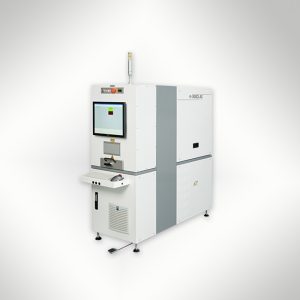
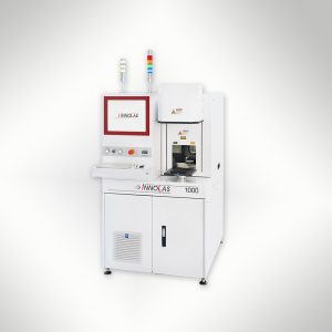
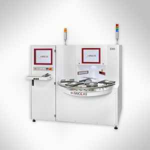
Semiconductor Processing Laser Systems
Semiconductor manufacturing demands exceptional precision, consistency, and traceability throughout the production cycle. Laser-based semiconductor processing systems provide unmatched accuracy for critical applications such as wafer marking and wafer sorting, which are essential for efficient production and quality control in the semiconductor industry. TLM Laser, in partnership with InnoLas Semiconductor, offers industry-leading solutions designed to meet the rigorous demands of this advanced sector.
Innovate with Confidence
Laser Machines and Systems for Semiconductor Processing

Talk to Us!
Connect with our Technical & Support Team.
Key Feature
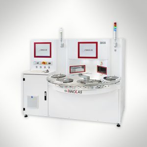
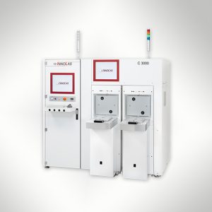
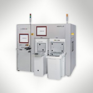
Wafer Marking and Sorting Excellence
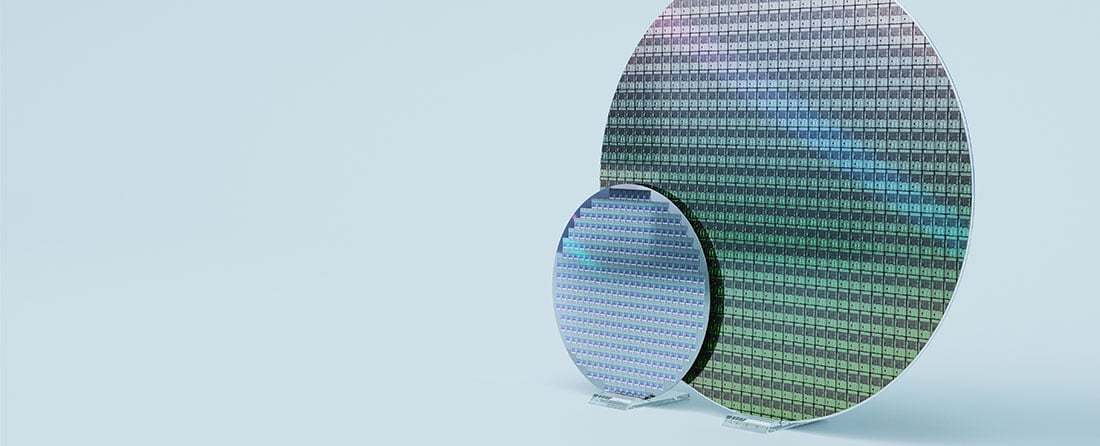
Wafer marking and sorting play a pivotal role in semiconductor manufacturing, where accurate identification and traceability are essential for maintaining production integrity. InnoLas Semiconductor wafer marking systems provide high-contrast, permanent marks for silicon wafers, ensuring traceability throughout the entire production process. Their wafer sorting solutions further streamline production by automating quality control, sorting & organising wafers based on critical metrics such as thickness, weight, and ID.
These systems are optimised for 300mm wafer production and can handle a variety of materials, including silicon carbide (SiC) and gallium arsenide (GaAs).
Explore our specialist wafer marking and wafer sorting systems to ensure seamless production processes in semiconductor fabrication.

Information About Semiconductor Processing Systems
Semiconductor processing relies on laser-based precision systems for handling sensitive materials with minimal risk of damage. These systems offer non-contact processing, ideal for delicate substrates and high-accuracy results.
Key Applications:
- Wafer Marking: Precision laser marking for traceability and identification on semiconductor wafers, ensuring compliance with international standards.
- Wafer Sorting: Automated systems for sorting wafers by thickness, weight, and identification, essential for production efficiency.
- Microstructuring: Fine material removal processes used in advanced packaging and micro-electronics.
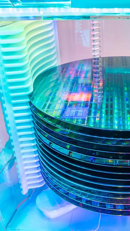
These laser solutions are particularly effective for silicon wafers, glass substrates, and other advanced materials used in integrated circuit manufacturing.
Answering Your Questions
Frequently Asked Questions
Both laser marking and wafer sorting are integral to maintaining high-quality standards in semiconductor production. Laser marking provides permanent identification of each component, enabling traceability and facilitating the tracking of products throughout their lifecycle. Wafer sorting ensures that only functional dies advance to the packaging stage, effectively filtering out defective units early in the process. Together, these processes help minimise errors, reduce waste, and ensure that only components meeting strict quality criteria reach the market.
Wafer sorting, also known as wafer testing, is a process performed during semiconductor fabrication where each die (individual chip) on a silicon wafer is electrically tested for functionality. The primary purpose of wafer sorting is to identify non-functional or defective dies before they proceed to packaging, thereby preventing the assembly of faulty components. This step is crucial for enhancing overall yield, reducing manufacturing costs, and ensuring the reliability of semiconductor devices.
Laser marking is a process that uses focused laser beams to create precise, permanent marks on materials. In the semiconductor industry, this technique is essential for inscribing critical information onto wafers. The high precision of laser marking ensures that even microscopic marks are clear and readable, facilitating effective traceability and quality control throughout the manufacturing process.
Reviews
Don’t Just Take Our Word for It
Our Customers


Talk to Us!
Connect with our Technical & Support Team.