
Wafer Sorting for the Semiconductor Industry
Optimise your semiconductor manufacturing process with precision wafer sorting systems designed to enhance efficiency, accuracy, and throughput. Our advanced solutions ensure seamless integration into your production line, maintaining the highest standards of quality and reliability.
The Importance of Wafer Sorting in Semiconductor Manufacturing
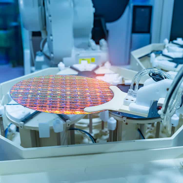
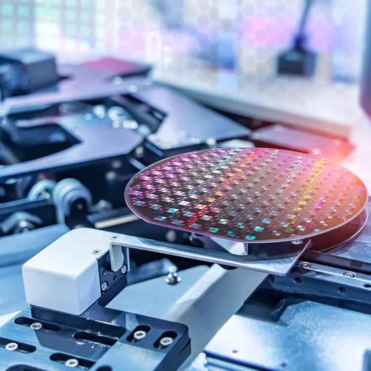
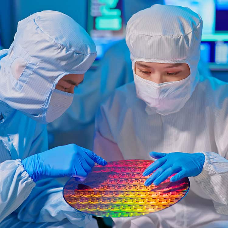
In semiconductor fabrication, wafer sorting is a critical process that involves organising wafers based on specific parameters such as ID codes, thickness, and weight. This meticulous categorisation is essential for:
- Process Optimisation: Ensuring that wafers meet precise specifications before advancing to subsequent manufacturing stages.
- Quality Assurance: Identifying and segregating wafers that deviate from desired parameters to maintain product integrity.
- Inventory Management: Streamlining the handling and tracking of wafers throughout the production cycle.
Effective wafer sorting minimises defects, reduces waste, and enhances overall production efficiency, making it indispensable in the semiconductor industry.


Applications of Wafer Sorting Systems
Wafer sorting systems are employed at various stages of semiconductor manufacturing to ensure that only wafers meet stringent criteria and proceed through the production process. Key applications include:
1. Sorting by ID:
Utilising advanced camera systems, wafers are identified by their unique ID codes and sorted accordingly. This facilitates:
- Ascending or Descending Order Sorting
- Splitting or Merging of Wafers
- Randomisation
- Individual Sorting Controlled by Host Systems
Such flexibility allows for customised sorting strategies tailored to specific production requirements.
2. Sorting by Thickness:
High-precision sensors measure wafer thickness to ensure compliance with process specifications. Wafers can be automatically sorted in ascending, descending, or randomised order based on thickness measurements, aiding in process adjustments and material verification.
3. Sorting by Weight:
Precision scales measure wafer weight with high accuracy. Sorting wafers by weight enables fine-tuning of processes such as etching, ensuring uniformity and consistency in production outcomes.
InnoLas Semiconductor’s Wafer Sorting Solutions
As a market leader in developing and manufacturing laser equipment for wafer marking and sorting, InnoLas Semiconductor GmbH offers a range of high-quality wafer sorting systems designed to meet the diverse needs of the semiconductor industry.
Key Features of InnoLas Wafer Sorting Systems:
Versatile Wafer Handling: Capable of managing wafer sizes from 2 inches to 450 mm, accommodating a wide range of semiconductor applications.
High Throughput: Designed for rapid sorting, with certain models achieving up to 300 wafers per hour in sorting mode and 600 wafers per hour in transfer mode, ensuring efficiency in high-volume production environments.
Cleanroom Compatibility: Manufactured and assembled in ISO 6 (ISO 14644-1) cleanroom environments, ensuring compliance with stringent cleanliness standards required in semiconductor fabrication.
Integration with Inspection Tools: Many InnoLas sorting systems function as fully automatic loading and unloading systems for inspection tools (EFEM), facilitating existing production lines.
Highlighted InnoLas Wafer Sorting Systems
IL 2600
Designed to merge, split, or sort wafers ranging from 2 inches to 200 mm by ID, weight, or thickness. Equipped with up to six input/output stations for open cassettes, it offers high throughput suitable for various customer requirements.
IL C3600
Engineered to handle 300 mm wafers, this system features up to five automatic FOUP load ports and operates within an ISO 3 mini-environment. It is suitable for PGV, AGV, and OHT loading, and can serve as a wafer transfer module in conjunction with measurement or inspection tools (EFEM).
IL C3800
Capable of splitting, merging, and sorting 300 mm wafers, the IL C3800 offers up to seven automatic FOUP load ports and maintains an ISO 3 mini-environment. It is designed for integration with various automated guided vehicles and overhead transport systems, enhancing automation in wafer handling.
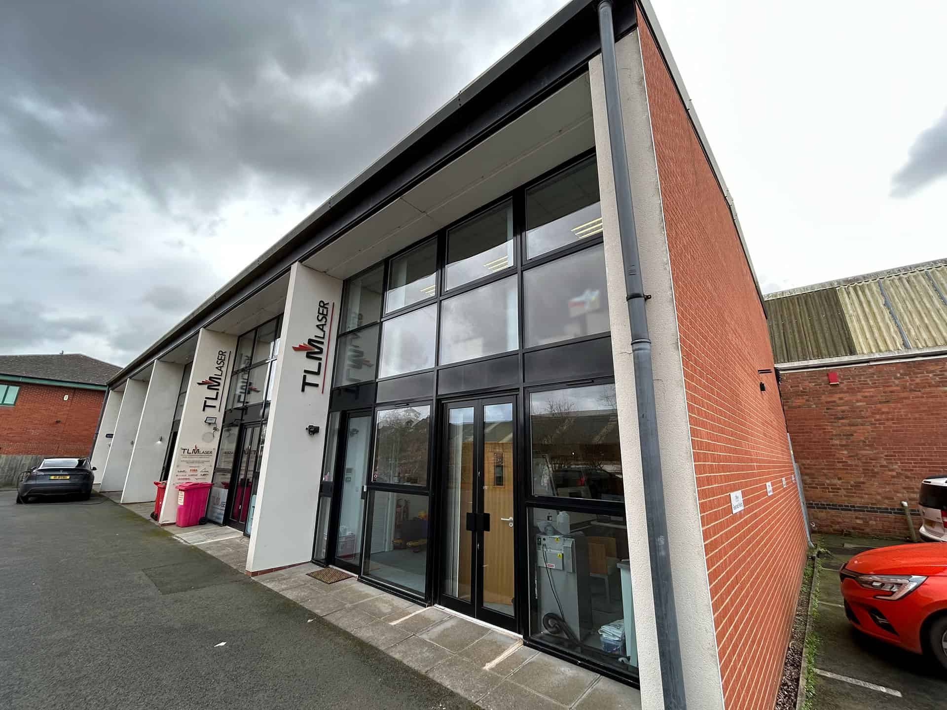
TLM Laser: Your Partner in Wafer Sorting Solutions
As the exclusive distributor of InnoLas Semiconductor systems in the UK and Ireland, TLM Laser provides comprehensive sales, service, and support for wafer sorting solutions. Our team of experienced engineers is dedicated to delivering:
Consultation and System Selection: Assisting you in choosing the optimal wafer sorting system tailored to your specific production needs.
Installation and Integration: Ensuring seamless incorporation of the sorting system into your existing manufacturing processes.
Training and Support: Providing thorough training for your personnel and ongoing technical support to maintain peak system performance.
Maintenance and Spare Parts: Offering prompt maintenance services and readily available spare parts to minimise downtime and sustain productivity.
Implementing state-of-the-art wafer sorting systems is pivotal for achieving precision, efficiency, and quality in semiconductor manufacturing. Partner with TLM Laser and InnoLas Semiconductor to leverage cutting-edge technology and industry expertise, ensuring your production processes meet the highest standards.
Answering Your Questions
Frequently Asked Questions
Reviews
Don’t Just Take Our Word for It
Our Customers


Blog Posts
Laser News & Information

Talk to Us!
Connect with our Technical & Support Team.