
Laser Marking for the Semiconductor Industry
Achieve precise, permanent identification and traceability of semiconductor wafers with advanced laser marking systems. Designed for efficiency, accuracy, and process stability, our laser solutions ensure seamless integration into high-volume manufacturing lines.
Why Laser Marking is Critical for the Semiconductor Industry
In the semiconductor industry, precision and traceability are essential for quality control, process stability, and regulatory compliance. Laser marking offers a non-contact, permanent marking method capable of producing high-contrast, durable marks on delicate semiconductor wafers. This level of precision ensures traceability throughout the entire wafer production cycle, from initial fabrication to the final stages of assembly and testing.
As the complexity of semiconductor devices increases, so does the demand for more precise and permanent identification methods. Laser marking not only ensures reliable identification but also plays a key role in quality assurance, batch traceability, and production monitoring in cleanroom environments.

Applications of Laser Marking in Semiconductor Manufacturing
Laser marking systems are widely used across various stages of semiconductor manufacturing, ensuring traceability and defect-free results. Key applications include:
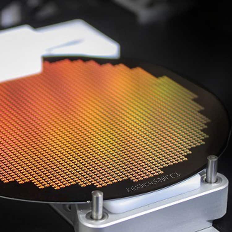
Wafer Identification and Tracking
Laser marking provides permanent serial numbers, batch IDs, and data matrix codes directly onto wafers. These marks can be scanned and read by both humans and automated systems, ensuring complete traceability during the wafer’s entire lifecycle.
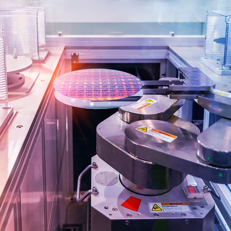
Quality Control and Sorting
Laser-marked wafers allow for automated wafer sorting and classification during quality control. With minimal surface alteration, the structural integrity of the wafer is preserved while ensuring high readability.
The Science Behind Laser Marking in Semiconductors
Laser marking in semiconductor manufacturing relies on high-precision laser sources such as Nd:YAG and CO₂ lasers to generate permanent, high-contrast marks on silicon and other materials. This non-contact process involves focusing a laser beam on the wafer surface, causing a controlled reaction that alters the material to create a legible, durable mark.
Key Laser Types Used in Semiconductor Marking:
- Nd:YAG Lasers (1064 nm): Ideal for creating precise, high-contrast marks on silicon wafers.
- CO₂ Lasers (10,600 nm): Often used for larger marks and barcodes with rapid processing capabilities.
- UV Lasers (355 nm): Suitable for ultra-fine marking on sensitive semiconductor surfaces with minimal heat impact.
Key Scientific Principles:
The laser beam generates localised heat, creating either material removal (ablation) or colour change depending on the laser type and wafer material. This ensures precise markings with minimal heat-affected zones (HAZ), critical in semiconductor manufacturing where material integrity is essential.
Key Benefits of Laser Marking for Semiconductor Wafers
1. Unmatched Precision for Nanometre-Scale Accuracy
Laser systems can create extremely fine, high-resolution marks that meet the semiconductor industry’s demanding accuracy standards, ensuring complete traceability without compromising wafer integrity.
2. Permanent, Tamper-Proof Markings
Laser-marked identifiers are resistant to heat, chemicals, and mechanical wear, making them ideal for long-term identification throughout the wafer’s lifecycle.
3. Non-Contact Process
The non-invasive nature of laser marking ensures minimal stress on delicate wafers, preserving their structural integrity while still achieving high-speed, accurate marking.
4. Consistency in High-Volume Production
Laser marking systems, such as those from InnoLas Semiconductor, are designed for high-speed marking in production environments, supporting both batch and continuous operation with minimal downtime.
5. Compliance with Semiconductor Standards
Laser marking ensures compatibility with industry standards, such as SEMI OCR and Data Matrix Codes, allowing seamless integration with commercially available scanners and inspection systems.
TLM Laser: Exclusive Distributor of InnoLas Semiconductor Systems
At TLM Laser, we are proud to be the exclusive distributor of InnoLas Semiconductor systems for the UK and Ireland. InnoLas is a leading manufacturer of precision laser systems for wafer marking and sorting, trusted by some of the world’s top semiconductor producers.
Why Choose InnoLas Semiconductor Systems?
- Proven Performance: Over 1,000 installations worldwide, ensuring field-tested reliability.
- Advanced Handling Technology: Systems with automatic alignment and edge grip handling for enhanced efficiency.
- Flexible Marking Systems: Support for various wafer sizes, from 2” to 300mm, with systems optimised for different materials and production scales.
- Minimal Downtime: Designed for maximum availability with fail-safe operation and industry-leading service support.
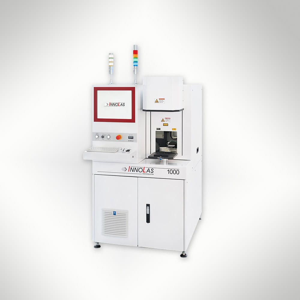
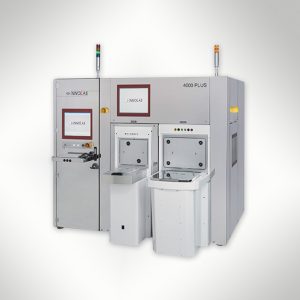
Key InnoLas Products for Semiconductor Marking
- IL 600 – Compact marking system for smaller wafers.
- IL 1000 & IL 2000 – High-precision systems for advanced marking requirements.
- IL 3000 – Designed specifically for 300mm wafers with full traceability features.
- IL C3000 & IL C4000 – Class 1 mini-environment systems with ISO 3 compliance for cleanroom use.
Why Partner with TLM Laser for Semiconductor Solutions?
Industry Expertise
Our engineers are globally recognised for their experience in the semiconductor sector.
Comprehensive Support
From consultation and installation to after-sales servicing and spare parts supply.
Training and Guidance
Full operational training to help your team integrate laser marking seamlessly.
Custom Solutions
We work closely with you to configure systems tailored to your production needs.
Answering Your Questions
Frequently Asked Questions
Reviews
Don’t Just Take Our Word for It
Our Customers
Blog Posts
Laser News & Information

Talk to Us!
Connect with our Technical & Support Team.