Laser Marking & Engraving for Electrical and Electronic Component Manufacturing
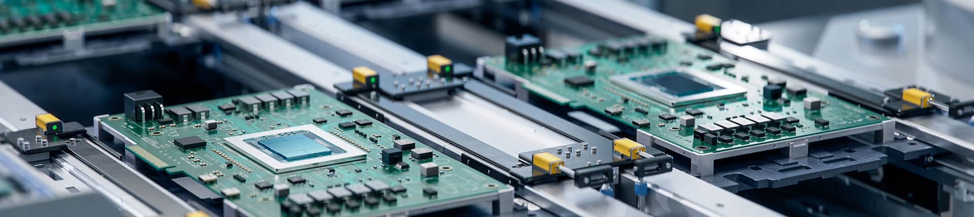
In the fast-evolving world of electrical and electronic component manufacturing, precision, durability, and compliance are essential. Laser marking and engraving provide unmatched solutions for component identification, traceability, and compliance, ensuring products meet industry standards while maintaining operational efficiency. From marking microchips to plastic connectors, laser technology offers a versatile, reliable, and cost-effective solution for manufacturers.
Applications of Laser Marking in Electrical and Electronic Components
Laser marking is widely used across the electronics industry to create permanent, high-quality identifiers. Common applications include:
Traceability:
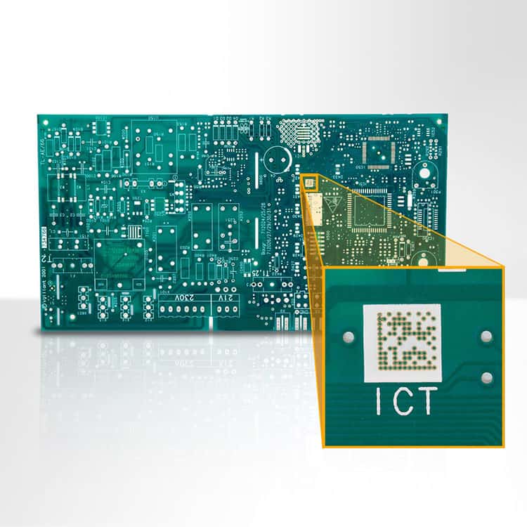
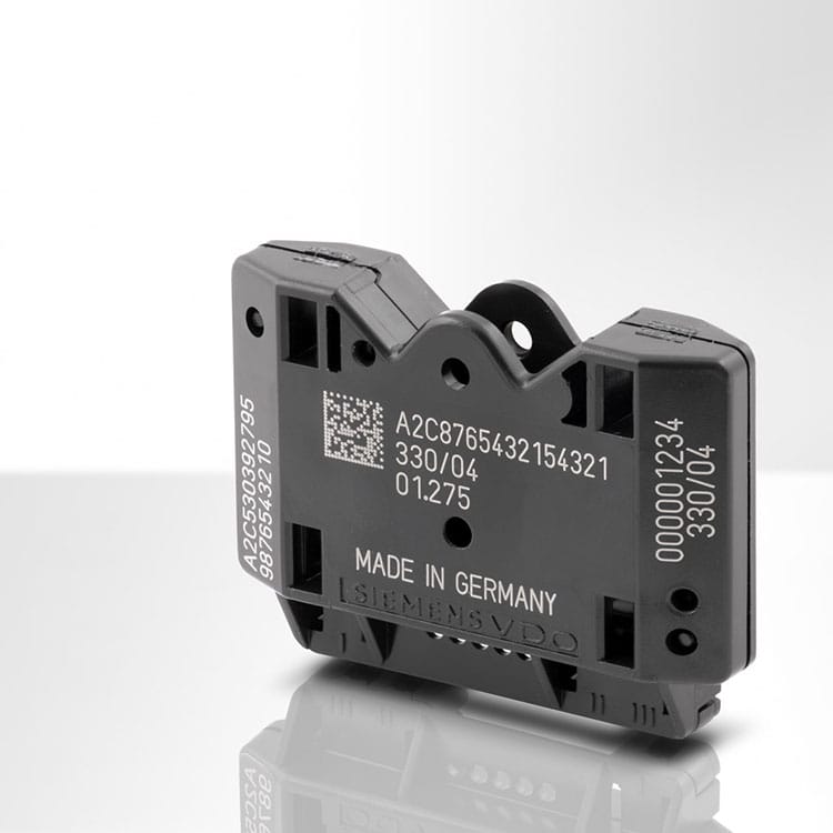
Serial numbers, QR codes, and barcodes allow manufacturers to track products through production and the supply chain, aiding in recalls, inventory management, and quality assurance.
Compliance Marking:
Ensure adherence to global standards like CE, RoHS, and UL by applying permanent compliance markings that are legible and resistant to wear.
Brand Protection and Anti-Counterfeiting:
Logos, batch codes, and unique identifiers prevent counterfeiting and protect intellectual property by providing tamper-proof, high-resolution marks.
User Information and Instructions:
Mark voltage ratings, connection details, or assembly instructions directly onto components, enhancing user safety and efficiency.
Inventory Management:
Laser-marked barcodes and QR codes streamline automated inventory tracking, improving supply chain efficiency.

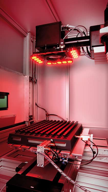
The Science Behind Laser Marking for Electronics
Laser marking involves using focused laser beams to interact with the surface of materials like plastics, metals, or ceramics. Depending on the application, the process may use techniques such as:
- Annealing: Produces smooth, high-contrast marks on metals without affecting the surface.
- Engraving: Removes material for deep, permanent marks on durable components.
- Ablation: Selectively removes coatings on multilayered parts like printed circuit boards (PCBs).
- Etching: Creates shallow, high-precision marks, ideal for small or intricate designs.
These methods ensure markings are resilient against wear, corrosion, and environmental conditions, making them ideal for long-term use in electronic components.
Key Benefits of Laser Marking in Electronics
Non-Contact Process:
The laser process does not apply physical stress, ensuring that delicate electronic components remain undamaged.
High Precision:
Lasers deliver accurate, detailed marks even on the smallest and most intricate components, essential for microchips and connectors.
Durability:
Laser marks are resistant to environmental factors, including chemicals, abrasion, and high temperatures, ensuring legibility throughout a product’s lifecycle.
Eco-Friendly:
Unlike traditional marking methods, lasers require no consumables such as ink or chemicals, reducing waste and environmental impact.
Speed and Automation:
High-speed lasers seamlessly integrate into production lines, enabling efficient, large-scale marking without compromising on quality.
Why Choose TLM Laser for Your Electronics Applications?
As the UK and Ireland distributor for FOBA, TLM Laser provides comprehensive solutions tailored to the electronics sector. Our expertise ensures seamless integration of FOBA’s advanced laser systems into your manufacturing processes. We collaborate closely with you to identify the best system for your needs, offering ongoing support and training to maximise efficiency and output.
Answering Your Questions
Frequently Asked Questions
Reviews
Don’t Just Take Our Word for It
Our Customers


Blog Posts
Laser News & Information

Talk to Us!
Connect with our Technical & Support Team.